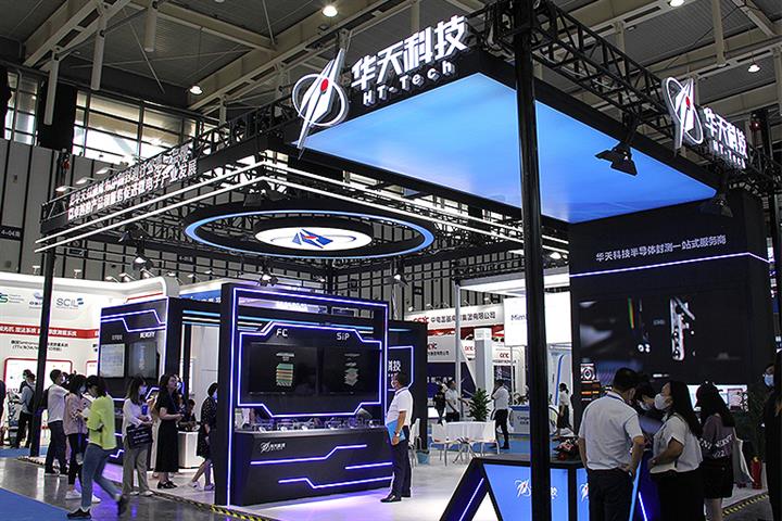
 China’s Huatian to Spend USD415.4 Million on New Cutting-edge Chip Packaging Plant
(Yicai Global) March 28 -- Chinese semiconductor packaging and testing firm Tianshu Huatian Technology plans to build a CNY2.9 billion (USD415.4 million) factory that will focus on the next generation of chip packaging processes that will be applied in emerging sectors such as Internet of Things and wearable devices.
The facility, which will be located in Nanjing, eastern Jiangsu province, will be able to package and test three types of integrated circuits, including 480,000 pieces of Wafer-level Chip Scale Packaging a year, the Tianshu, northwestern Gansu province-based firm said yesterday. It will focus on the advanced packaging process, which is currently very much in demand and has a promising outlook
Chip sizes are getting so small that it will soon not be possible to make them any smaller. This leaves considerable room for packagers to develop cutting-edge technologies that will help improve chip properties, it said.
The new plant is expected to generate CNY266 million (USD38.6 million) in net profit a year and revenue of CNY1.3 billion (USD183.1 million) once it is up and running, Huatian Technology said. Construction should start in June and will finish by June 2028. Production will gradually start as the facility is being built to enhance efficiency.
The company has been affected by weak demand and sliding profitability in the chip sector. It logged a 46.7 percent plunge in net profit last year from the year before to CNY754 million (USD109.5 million), while revenue dipped 1.5 percent to CNY11.9 billion (USD1.7 billion), according to its latest financial report released yesterday.
Last year, Huatian Technology packaged 41.9 billion chips, a dive of 15.6 percent year on year. Of this, 1.3 million were wafer-level integrated circuits, a decline of 3.1 percent. Huatian Technology’s share price [SHE:002185] closed down 2.4 percent at CNY10 (USD1.46) today.
Editor: Kim Taylor