 China Electronics Engineering Design Institute Denies Country Is Building EUV Lithography Machine Plant
(Yicai) Sept. 19 -- The China Electronics Engineering Design Institute has refuted rumors claiming the country is building a plant to produce extreme ultraviolet lithography machines, which are used to pattern the finest details on the most advanced chips.
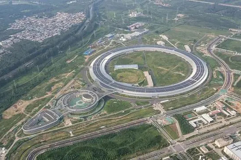
The picture recently circulating online does not show an EUV lithography machine plant but a high-energy photon source project under construction in Beijing’s Huairou district, the CEEDI said yesterday.
According to a recent online rumor, Tsinghua University has managed to giantize Advanced Semiconductor Material Lithography’s lithography machine through an extreme ultraviolet project in Beijing’s neighboring Xiong’an New Area, achieving homegrown production.
The HEPS project in the picture is China’s first ever and has the world’s brightest fourth-generation synchrotron radiation light sources, the CEEDI noted, adding that it started construction in 2019 and is expected to come on stream by the end of 2025.
The project is a collaborative effort of the design team led by State Development and Investment’s Chief Scientist Lou Yu and several scientific research and design teams of the CEEDI.
A HEPS is an ultra-precise, ultra-high-speed, giant X-ray machine that generates small beams that can penetrate matter for three-dimensional scanning to observe molecules and atoms, the CEEDI explained.
Editor: Futura Costaglione